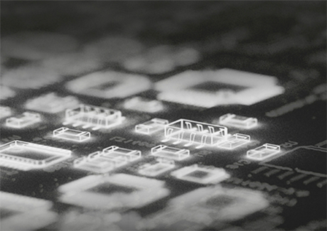
A printed circuit board (PCB) or printed wiring board (PWB) is a laminated sandwich structure of conductive and insulating layers. PCBs have two complementary functions. The first is to affix electronic components in designated locations on the outer layers by means of soldering. The second is to provide reliable electrical connections (and also reliable open circuits) between the component’s terminals in a controlled manner often referred to as PCB design. Each of the conductive layers is designed with an artwork pattern of conductors (similar to wires on a flat surface) that provides electrical connections on that conductive layer. Another manufacturing process adds vias, plated-through holes that allow interconnections between layers.
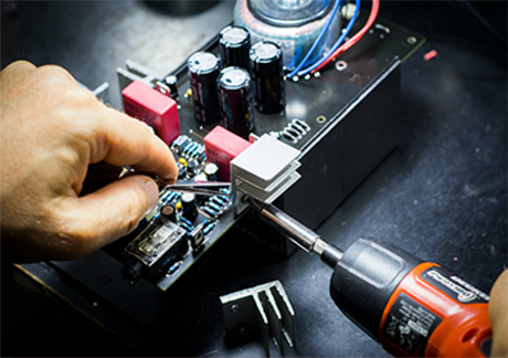
PCBs mechanically support electronic components using conductive pads in the shape designed to accept the component’s terminals, and also electrically connect them using traces, planes and other features etched from one or more sheet layers of copper laminated onto and/or between sheet layers of a non-conductive substrate. Components are generally soldered onto the PCB to both electrically connect and mechanically fasten them to it.
Printed circuit boards are used in nearly all electronic products. Alternatives to PCBs include wire wrap and point-to-point construction, both once popular but now rarely used. PCBs require additional design effort to lay out the circuit, but manufacturing and assembly can be automated. Electronic computer-aided design software is available to do much of the work of layout. Mass-producing circuits with PCBs is cheaper and faster than with other wiring methods, as components are mounted and wired in one operation. Large numbers of PCBs can be fabricated at the same time, and the layout only has to be done once. PCBs can also be made manually in small quantities, with reduced benefits.[2]
PCBs can be single-sided (one copper layer), double-sided (two copper layers on both sides of one substrate layer), or multi-layer (outer and inner layers of copper, alternating with layers of substrate). Multi-layer PCBs allow for much higher component density, because circuit traces on the inner layers would otherwise take up surface space between components. The rise in popularity of multilayer PCBs with more than two, and especially with more than four, copper planes was concurrent with the adoption of surface mount technology. However, multilayer PCBs make repair, analysis, and field modification of circuits much more difficult and usually impractical.